
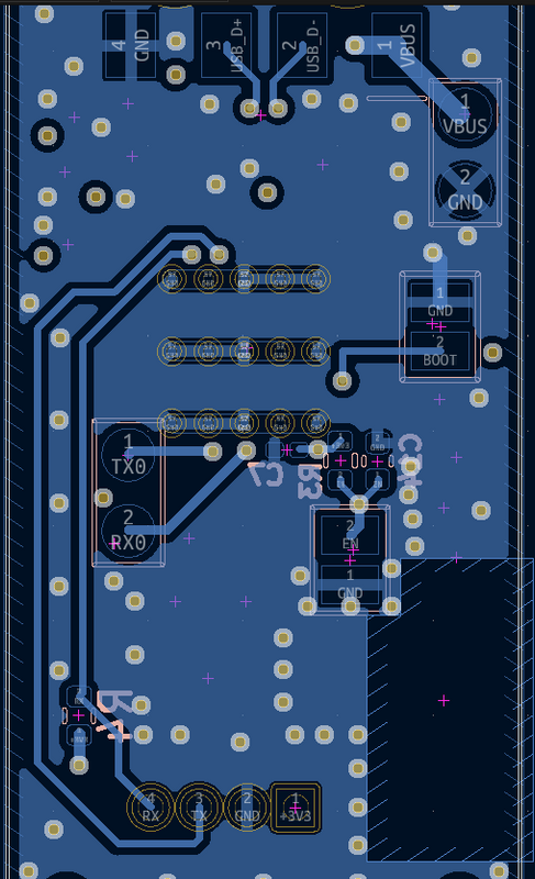
The purpose of this PCB is to be small, have ok RF performance, and use USB as main power-source and interface. (Off course it has UART if USB is not available) this is just a somewhat challenge I set myself to design a esp32 PCB with the IC without a already made module.
Link to gallery: https://postimg.cc/gallery/HnVZxSX Excuse the quality of the images, Im quite new to exporting PCB from kicad.
Depending on the power consumption, you may consider not using thermal relief while connecting thermal vias for the chip (component 57) to ground layers. But this may make soldering harder so do it only if needed. Thermal vias are so close that they form 3 long dents in 3v3 plane. It is good practice to put vias a little far apart so that planes can go through between vias. This can be important since sometimes lowest impedance can be obtained when current is flowing between those vias. If you don’t need to fit 15 vias there, you may consider reducing the number and separating them a bit. You can also check the design rules for minimum copper width and minimum via clearance for your manufacturer and enter them in your CAD tool.