
cross-posted from: https://lemmy.world/post/5214451
Hey everyone,
I’ve noticed your community has sprung up somewhat recently. I was making posts at !microcontrollers@lemux.minnix.dev, but figured I’d share my most recent post here.
I’ve created 5 tiers, from 0 (cables), to 4 (BGA/Transmission Lines), which roughly categorize modern hobbyist electrical engineering / PCB design skills. Knowing the rough skill levels should help beginners choose what they want to study and what they want to work towards.
Beginner Series I: What is a Microcontroller https://lemux.minnix.dev/post/10943
Beginner Series II: The “Generic” Microcontroller https://lemux.minnix.dev/post/23245
Beginner Sidenote: Microchip’s Signal Chain Design Guide https://lemux.minnix.dev/post/64811
In my earlier writing, I’ve got this vague idea of “simple” and its opposite: “complexity”. This topic will help try to clarify this subject, because it will help the beginner decide what you want to study. Electronics can be as simple, or as complex, as you want to make it.
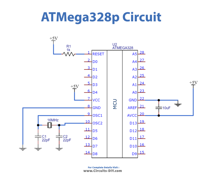
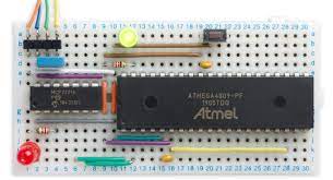
On the simplest end, we have chips like the ATMega328p which requires almost no components to boot up and function. In fact, that crystal on the bottom left? Optional. People have used breadboards or 1-layer PCBs to make usable designs with this chip.
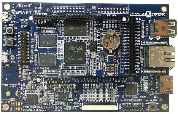
However, when we reach into the realm of microprocessors, such as this SAMA5D4, the shear number of components… and the high skill needed to layout a 10-layer PCB (BGA Fanout, Impedance-matched traces, Power-delivery networks) gets damn close to Masters-degree level of skill and training to fully understand.
Choosing the level of complexity you want to work with (and what level you wish to study up to) is all up to you, and is one of the most rewarding parts of this hobby.
Tier 0: Wires and Connectors
At the absolute simplest level is what I like to call “Lego Electronics”. You either build computers by buying premade connectors, boards, or motherboards, and plugging them together as if they were expensive Legos.
This is great! The years have brought many useful products and experiments you can do today without ever learning about any electrical engineering.
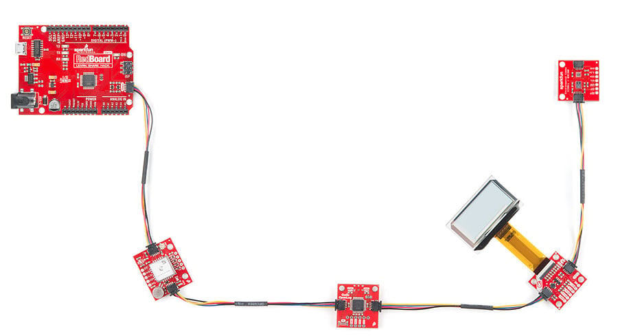
Sparkfun has a system of wires and connectors called “Qwiic”. There’s no soldering involved, just a bunch of wires in standard “JST” connectors. You buy premade parts and just click them into different systems.
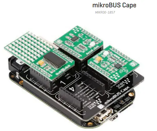
Nonetheless: wires and connectors remain a necessary skill for all electronic hobbyists. And besides, everyone needs to start “somewhere”. There are a great many systems like this from a wide variety of competitors. Mikroe has their “Mikroe Click”, with board-to-board connectors just clicking into each other.
Or Arduino Shields, or Rasp. Pi Hats. There’s so many “Skill-free” connectors that anyone and everyone could get into the hobby today.
Note: Tier 0 is deceptively simple. Electrically speaking, yes, wires and connectors are really simple. In practice… they are not. There’s mil-spec connectors, high-current connectors, shielding, twisted pairs, a near infinite number of pins, headers or sockets that you’d have to deal with. All of which have different properties, pros/cons, downsides, EMI implications, noise implications and more. The more you advance in EE-knowledge, the more-and-more you’ll find yourself returning to Tier0 and learning more about it.
Case in point: go ask any experienced house electrician about when you should use Stranded AWG14 wire vs solid AWG16 wire and they’ll likely talk your ear off for an hour. Its a seriously complex question when you think about all the details and implications. This one is more flexible, that one carries more current, that one crimps easier but this one solders better. This one handles high-frequencies better due to skin-effect, that one doesn’t. Etc. etc. etc.
Fortunately, beginners will be dealing with low-power, low-speed circuits with little regards to EMI (electromagnetic interference) problems, mechanical strength problems, or heat / fire-safety problems. Connectors and wires could be complex, but I expect that most beginners in the 3.3V desktop-part world will have connectors so short, so small, and for hobby purposes only (no one is trying to sell these in a marketplace, right?), that we can just ignore all the parts that make wires / connectors complex and focus our attention on the other skill issues.
Maybe I’m mistaken though, so I’ll leave this note just in case. I expect some electrician would get angry at me if I didn’t point out that yes… electricians have to learn a lot of things with wires and connectors and can make an entire career out of this subject alone.
Don’t consider “Tier 0” the easiest. Consider “Tier 0” the most fundamental. I don’t care who you are: at all skill levels, you will run a wire from something, to something else. At that point, you’re dealing with “Tier 0” wires/connector issues and you damn well hope that you know what you’re doing. Did you use a shielded cable? Or a twisted pair? What are the pros/cons of such an approach? Etc. etc.
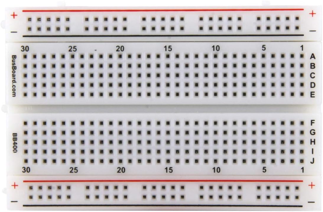
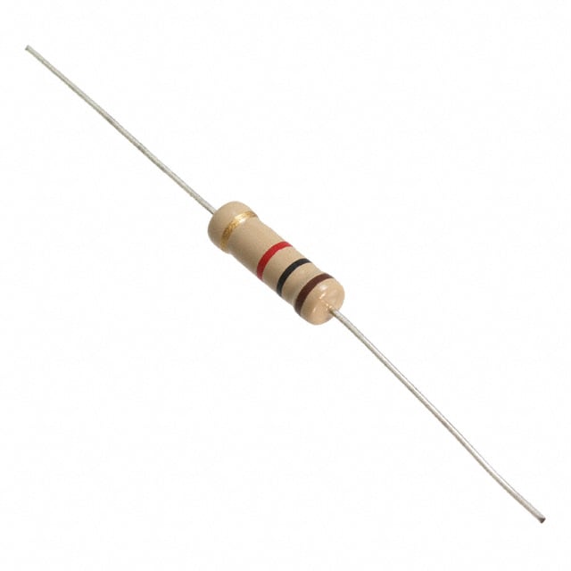
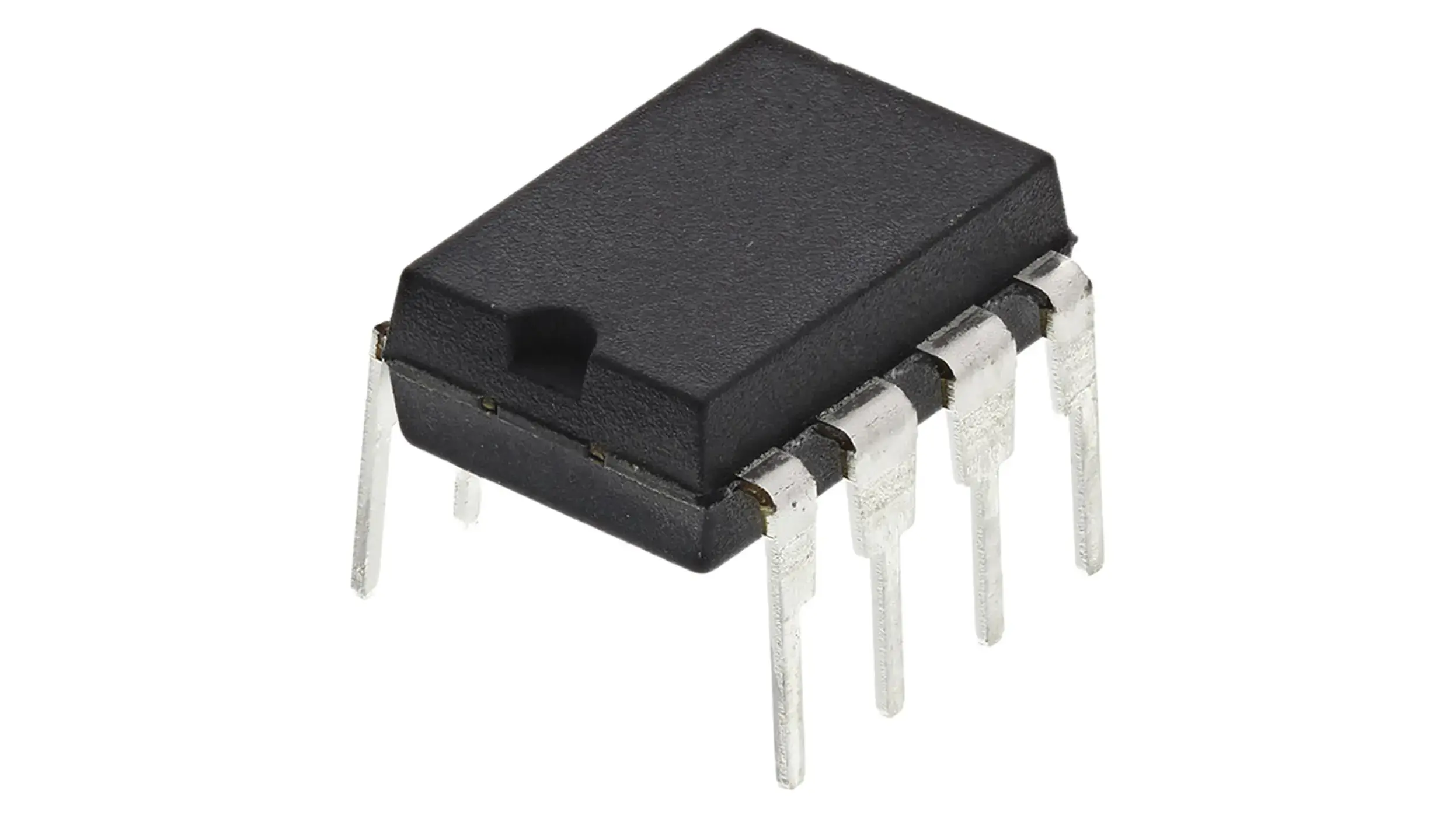
Tier 1: Breadboarding and Through Hole parts
In Electrical Engineering school, the breadboard is your first step forward. Each hole inside this breadboard has little springs that “grab” your electronics, while a wire across the springs will connect your electronics together.
You’ll buy through-hole components like the resistor above, or PDIP chips. These easily plug into a breadboard. And all together, you’ll be able to make something.
Alas, breadboards are basically trapped in the 1980s level of technology. While some companies, like Microchip, continue to make at least some new chips compatible with Breadboards (or more accurately: “through hole” design), the vast majority of chips are only available at “higher skill levels”.
Any “wire” can plug into a breadboard, meaning all items from Tier0 remain fully compatible with Tier1 with enough jumper wires and cables.
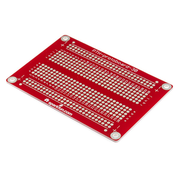
For a more “permanent” design, you can buy “Solderable Breadboards”. Such as this one from Sparkfun: https://www.sparkfun.com/products/12070
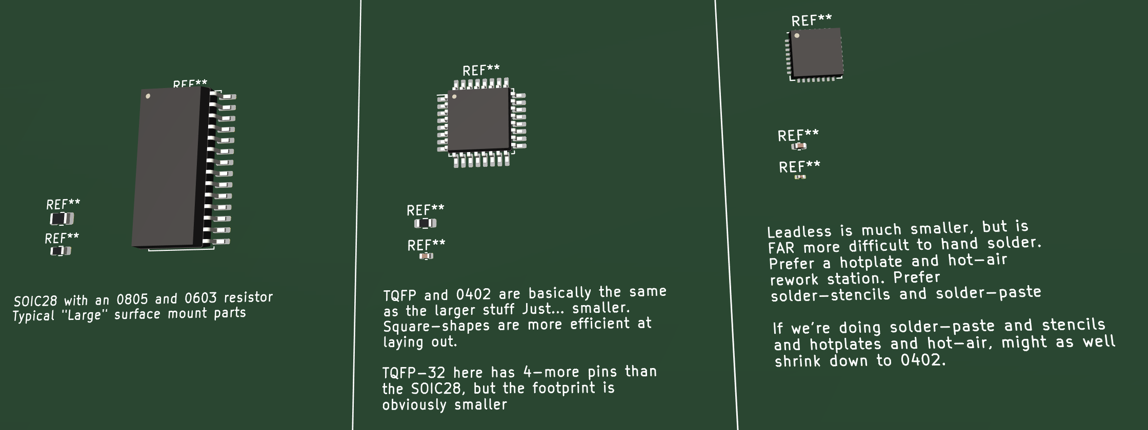
Tier 2: Low-speed “Large” Surface Mount custom PCBs
Note: Hobbyists can begin at this tier if they so choose !! Though more complex than Tier0 and Tier1, Low-speed Surface Mount PCBs has the widest selection of parts and much, much cheaper chips in practice.
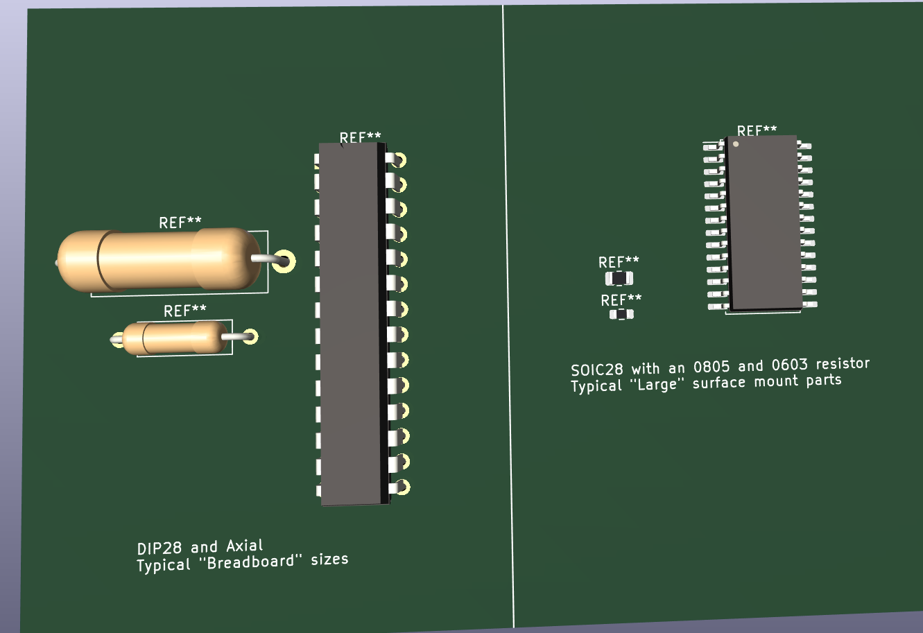
Breadboards and 0.1" pitch through hole parts are just too large, and all that extra plastic costs money. Shrinking down to SOIC or SOT sizes just makes sense. I’ve created this simulation in KiCAD to show the size difference.
When making your own PCBs, you’ll need to learn how to use a PCB-designer, such as KiCAD. KiCAD has a multi-step process: 1. Create Symbols. 2. Create Schematic using Symbols. 3. Assign Footprints to Schematic. 4. Create PCB design using Schematic+Footprints.
Because each of these 4 steps is a new skill to pickup, you’ll likely find yourself frustrated as you work with the program and try to learn. Still, once you learn the skill of PCB-layout, your productivity will skyrocket!!
While Breadboards and Wires get complex when you have more than a few dozen wires running around… PCBs have a computer layout thousands of wires at a time. All you have to do is solder the right parts to the correct location. At least… at this “low speed” level of skill.
With $5 per Sq. Inch PCB available today, I think all beginners can easily reach this skill-level of 0805 resistors + “large” SOIC surface mount chips.
Note: IMO, 2, 4, and 6 layer PCBs are all of similar studying / skill complexity. Its not the number of layers that make things difficult… its the electrical design itself. That being said, you can likely solve all your problems with just 2 layers only.
Tier 3: Beyond 20MHz and Leadless Chips
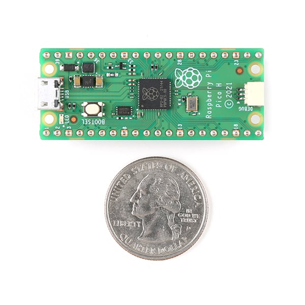
No, I’m not saying “buy a Rasp. Pi Pico”. I’m saying MAKE a Rasp. Pi Pico from scratch!! You can see the RP2040 leadless package right there front and center! However, if you plan to run the RP2040 at higher speeds, you might be surprised at what happens without some careful study…
With leadless, we’re beginning to reach into 1990s levels of technology here!
Above 20MHz or so, the larger 0805 capacitors are going to act more like resistors or even inductors (!!!) than proper capacitors. We’ve literally reached the frequency limits of the larger parts, and have to think more carefully about the weirdness of high-speed circuits. In ELI5 terms… this means that 0805 capacitors are physically too slow to provide power to electronics. You might see a brownout within the ~10 nanoseconds when a part like the RP2040 draws power on the start of a clock-tick.
Leads to your chips having too many parasitics? Cut them off and use leadless packages instead. 0805 has too much inductance? Switch to 0402 or even 0201 capacitors instead.
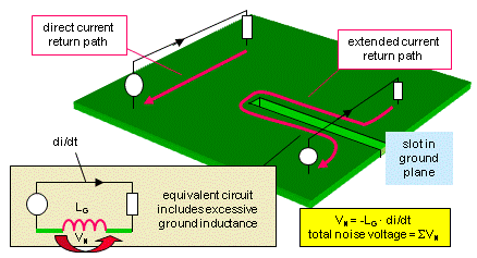
With these issues, 4-layer boards become mandatory. A “Power-plane” and “Ground-plane” allows you to easily visualize (well, in your mind’s eye) the current-loops that occur in your board. Ground loops after all create inductors. (Any “looped path” creates an inductor… which acts as an antenna… radiating noise out to other parts. And also an… inductor, which resists current changes and slows down your circuit, possibly making 20, 30, 50 or 100MHz speeds impossible).
Note: I’ve exaggerated a little bit. While parasitics are a concern, plenty of people still choose TQFP (leaded) packages at this level. But my overall point remains set: its necessary to learn about “clean PCB design” and good habits. With enough small decoupling capacitors and a bit of thought into simple Power-delivery networks like a ground plane + power-plane, you’ll get through this tier just fine.
The bulk of the “complexity” is honestly the physical issues you get when working with such small parts. Regular soldering becomes difficult and you really need to learn solder paste + solder stencils if you want to be comfortable with 0402 or smaller parts. Soldering irons are just barely possible though, even with leadless parts, if you really want to try. But seriously consider solder paste + stencil now.
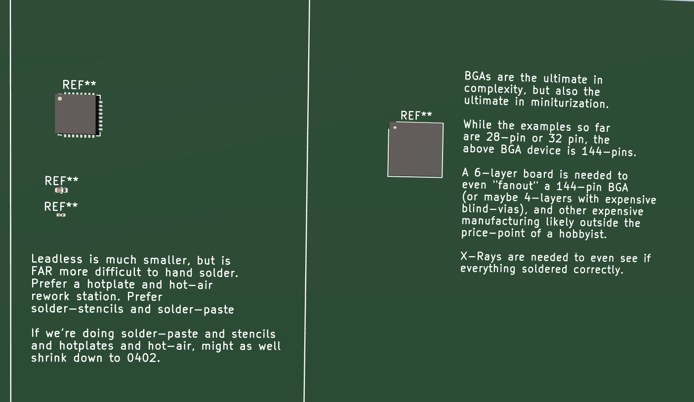
Tier 4: Transmission Lines and BGAs
BGAs offer the ultimate package density, but also the ultimate levels of complexity. Just routing the signals out of a BGA is difficult enough, but many BGA components are also some of the most complicated available on the market.
As all the connections of a BGA are “under” the chip, it often requires X-ray equipment to even see if the soldering job was done well.
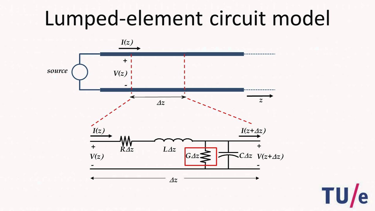
Your nightmares over parasitics only grows deeper. Due to extremely high (300MHz+) circuit speeds, you’ve begun to worry about exceptionally complex noise issues. You see every trace as a transmission line, and need carefully controlled and matched impedances to make sure that all your signals are reaching the DDR2 RAM chip at the same noise/attenuation/speed as all other lines.
https://www.analog.com/en/design-center/glossary/impedance-matching.html
You’ll likely need 6-layers to even think about using a BGA due to the “fanout” issue alone. Microchips SAMA5D4 reference design uses 10-layers for example. However, with OSHPark offering 6-layer boards (albeit without blind-vias) for $15 / sq-inch minimum-order 3 boards, BGAs have entered the realm of modern hobbyists.
Albeit with some advanced skills and knowledge, but yes. BGAs are within the hobbyist’s ability today, at least the “coarse” 0.8mm pitch BGAs. “Fine” 0.5mm or 0.35mm are beyond the hobbyist’s budget but if you’re seriously considering this you probably knew that already!
The soldering iron is literally impossible now. Only reflow techniques like a hotplate + hot air gun can even solder a BGA. If you need to “rework” a BGA, you might need to buy “solder balls” to rework BGAs.
Tier 5: Beyond?
The most modern tech today from the most advanced labs are doing “advanced packaging”, such as stacked RAM (such as HBM RAM), or die-to-die connections. But you probably work in one of the top labs in the world, so you probably don’t need this topic anymore!

You must log in or register to comment.